Hardware photographs
Photographs of the inside of a scanner, taken for this reference, so that claims about the hardware can be checked rather than taken on trust. They also give an owner something to compare against when they open their own machine.
Everything on this page is one F-135+, serial 16402, photographed from the component side of its main board on 24 August 2026. Getting to that view needs the bottom plate off, which is four security screws, with the scanner unplugged. Nothing here requires the scanner to be powered, and there is no reason to power it with the plate off.
What is missing
Most of the scanner. Nothing below has been photographed, and none of it can be inferred from what has:
- The CCD board. The most valuable gap. Its part number would give the
sensor's total and masked pixel counts from a datasheet, which bears
directly on the
Offsetquestion in calibration. - The light board, which differs between the two models: the Plus has a thermoelectric cooler and temperature sensing the base F-135 lacks, which is why their LED current ceilings differ.
- The motor board.
- The reverse of the main board, so whether the two EEPROMs below are the only ones in the scanner is not known.
- Any base F-135. Its main board is PCB #125039A, a separate design rather than a revision of the one here, so no part or marking on this page can be assumed to apply to it.
- The DX sensor area, where an open question about which detectors read the barcode is still unresolved (see DX barcode).
The main board
PCB #125430 REV C, marked © 2005 PAKON, INC.
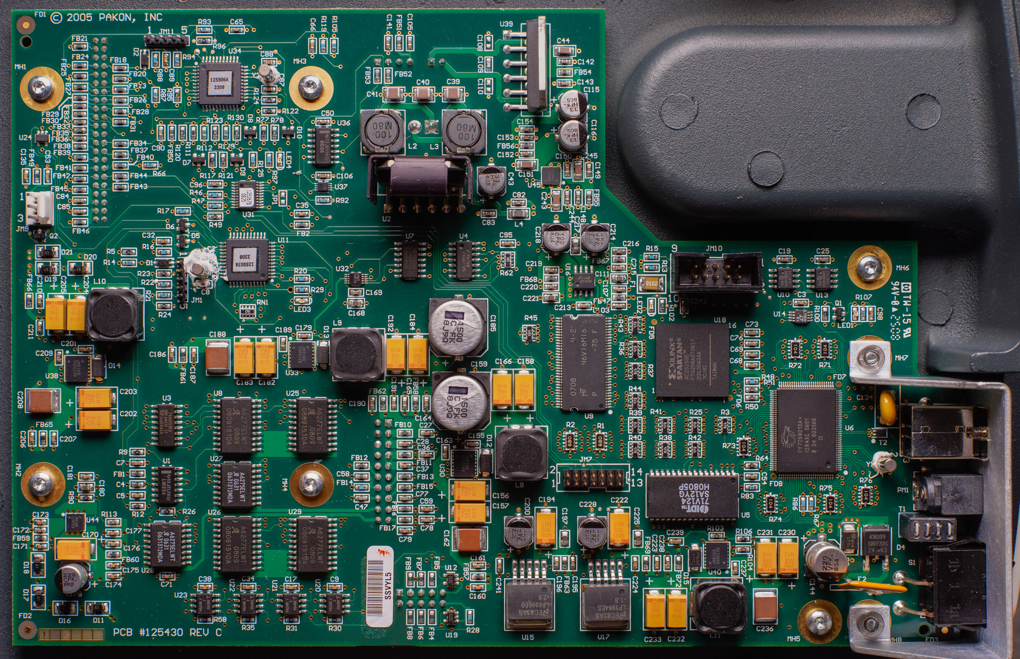
The board number
Silkscreened along the bottom edge. This is the marking to check before
reflashing a controller, because the OEM images are tied to it: 125430A,
125430B and 125430C take hardware versions 03, 04 and 05
respectively, and the base F-135's 125039A takes 02. Putting a Plus image
on a base board is the case the OEM readme warns about in capitals. See
per-unit data and safety.

The USB bridge
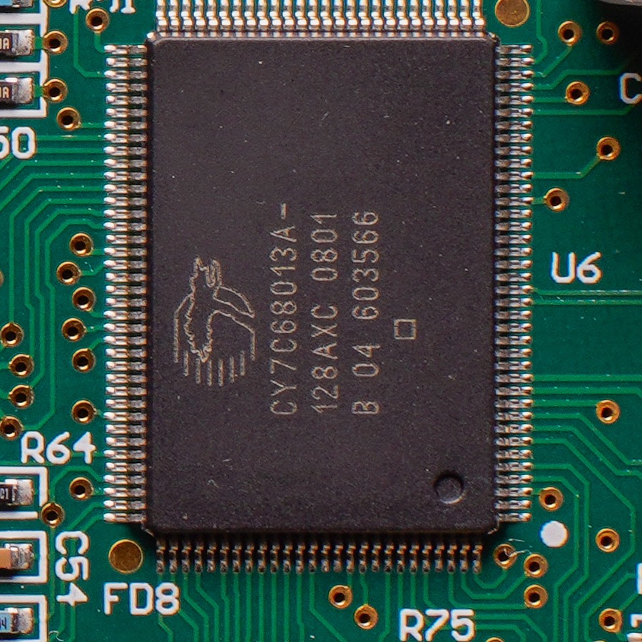
U6, a Cypress CY7C68013A-128AXC: the EZ-USB FX2LP in the 128-pin
package, date code 0801. It sits on the right of the board, below and right
of the FPGA, with its crystal alongside. This is the bridge everything the
host does passes through, described in
USB identity and firmware.
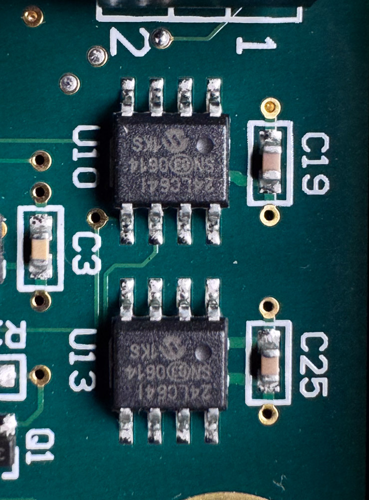
The two I2C EEPROMs
U10 and U13, above the FPGA near the top right, both marked
24LC64I / SN 0614 / 1KS. A 24LC64 is 8192 bytes. These are very likely the
chips answering at 0x51 and 0x52, though a photograph cannot say which
designator carries which address, and the strapping that decides it is not
readable here. The consequence for anyone archiving a scanner is on the
per-unit data and safety page: if the
capacity is right, only a small part of either chip has ever been read.
The round dot on each package marks pin 1, and the address is set by strapping
pins 1, 2 and 3. Traces from each chip run to the decoupling capacitor beside
it, C19 for U10 and C25 for U13, and the two are wired differently,
which is what two addresses on one bus requires. Which is which has not been
worked out; it would take a continuity check rather than a photograph, and
nothing in the software depends on the answer.
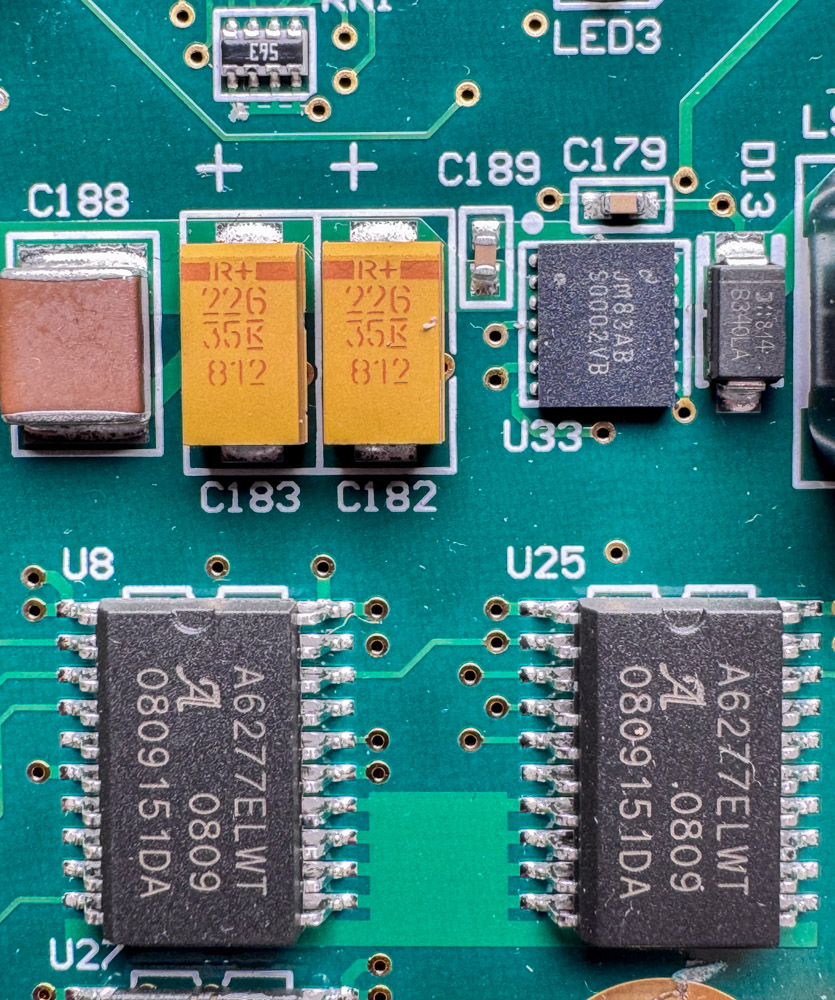
Driving the light
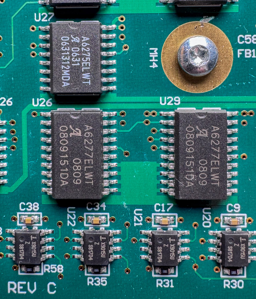
Five Allegro serial-input constant-current LED drivers sit on the main board,
not on the light board: A6277ELWT at U8, U25, U26 and U29, and an
A6275ELWT at U27. So the illuminant is driven from here, through the
connector, rather than by the light board's own controller.
Below them are four X9015U digitally controlled potentiometers at U20,
U21, U22 and U23, each with a 1001 resistor alongside. U23 is the
leftmost and sits rotated a quarter turn from the other three, so its marking
reads horizontally where theirs read vertically. Four of them,
on a scanner with four light channels, is a coincidence worth writing down: the
OEM keeps Current_R, Current_G, Current_B and Current_Ir per resolution
base and film mode, and a constant-current driver of this family sets its
output from an external resistance. A digital pot in that position would be how
a commanded current becomes an actual one.
That is a reading of the layout, not a traced circuit. Nothing here has been followed with a meter, the pots could as easily trim the A/D rather than the LEDs, and the count could be coincidence. [INFERRED, and weakly: from the part functions and the channel count only.]
The FPGA holds nothing when it is off
Spartan-IIE is SRAM-based, so U18 has to be given its bitstream every time
the scanner powers up, exactly as the FX2 is given Pakon7.hex. There is no
configuration PROM beside it, and the FX2 image is far too small to contain a
150K-gate bitstream, so the configuration arrives from somewhere else. The OEM
package carries a "CCD FPGA file" alongside its controller images, which is the
obvious candidate but is not documented here yet.
The consequence for the rest of the reference: the scan-window and gain registers described in calibration are registers in logic the host itself loads, not fixed silicon. Whatever those banks mean is a property of the bitstream in use.
Power
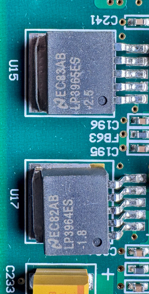
U15 is an LP3965ES-2.5 and U17 an LP3964ES-1.8, National low-dropout
regulators supplying the 2.5 V and 1.8 V rails the FPGA and memory need.
Also identified
Read off the same board, without a photograph good enough to reproduce here:
| Designator | Part | What it is |
|---|---|---|
U39 |
LMD18200T | National 3A/55V H-bridge, the transport motor driver |
U9 |
Micron MT46V16M16P-75 F |
256 Mbit DDR SDRAM, date code 0708 |
U5 |
IDT 71V124 SA12YG |
1 Mbit SRAM, date code H0805P |
U18 |
Xilinx XC2S150E, FTG256, speed 7C/6I |
Spartan-IIE FPGA, 150K system gates, 256-ball BGA. The scan-window and gain register banks live behind it |
U34, U11 |
125506A, 125507A, both dated 2208 |
44-pin QFPs whose Pakon number is printed on a white label stuck to the package, not moulded or laser-marked into it, which is why neither carries a manufacturer logo. The original marking is probably underneath. U11 has a second line whose lower edge is just visible and could not be read |
D13 |
B340LA |
Schottky rectifier |
Marks that have been read but not identified, in case someone recognises one:
| Designator | Mark | Note |
|---|---|---|
U14 |
LTBBW e3 |
Linear Tech logo. A top-mark code rather than a part number, so decodable from LTC's marking list by anyone who has it. Nothing else is printed on the package |
U33 |
JM83AB over SOOO2VB |
National logo, 16-pin. The second line is where a part number belongs but does not resemble one, so this may be house-marked like U34 and U11. Read as letter O rather than zero, though the two are hard to tell apart on a chip mark |
U16 |
CJAB 2995M |
National logo, 8-pin, beside the DDR |
| (bottom right) | X30 over UF400 |
a vertical part, logo like two overlapping Vs |
JM83AF on the U39 motor driver and JM83AB on U33 share a prefix, so
that field is a National lot code rather than part of either part number.
Contributing
Photographs of anything under what is missing would be welcome, the CCD board most of all.
Photographs here are by Ali Bosworth (alibosworth) and carry the same CC BY 4.0 licence as the rest of the reference. Contributed photographs need to be compatible with that.